| PTCOE's Capabilities at Georgia Tech |
![]()
| PTCOE has advanced thin-film deposition facilities which
include CVD, electron beam and sputtering systems, MBE/VPD and a large-area
Ion Assisted Deposition (IAD) systems. PTCOE's research faculty have extensive
experience in the deposition of inorganic materials by metalorganic and
molecular beam epitaxy as well as e-beam and thermal evaporation processes.
These systems have been used to deposit all types of materials such as
SrS:Cu,Ag, SrS:Ce, ZnS:Mn, CaS:Cu, SrGa2S4:Ce, LaO2S:Tb,
GdO2S:Tb, Si, InAlGaAsP, HgZnCdTe for displays and optoelectronic
device applications. These deposition capabilities are complemented by
insitu control and characterization techniques such as reflectance, reflection
high energy electron diffraction, residual gas analysis, quadrupole mass
spectrometry and auger electron spectrometry. Also, growth enhancement
capabilities are available including photoassisted deposition and ECR plasma
sources.Extensive expertise in the optical and electrical doping of these
materials has been developed. PTCOE's deposition systems have the capability
to handle low and high vapor pressure materials using conventional solid
source evaporation, valved crackers and gas sources (organometallics and
high pressure gases). In addition, several unique delivery systems have
been developed, which allow precise control over very high vapor pressure
materials and gas sources with control of flows over 6 orders of magnitude.
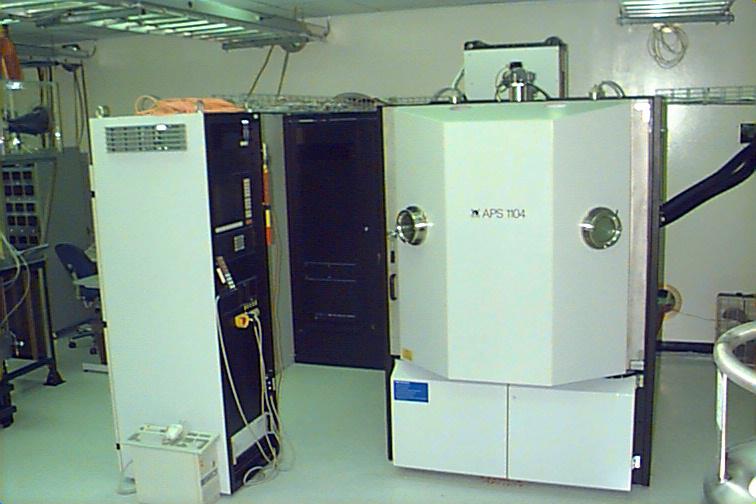
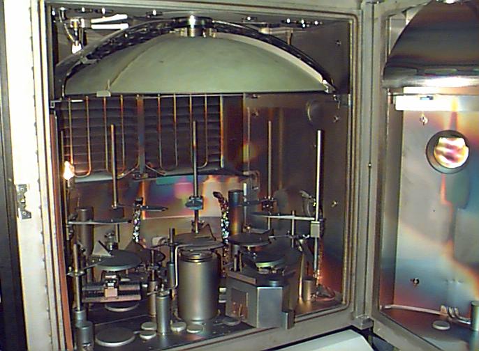
PTCOE's large-area IAD system allows the simultaneous co-evaporation
of four materials (thermal and electron beam) and the low temperature deposition
of high quality oxide materials.
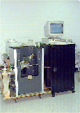
Summary of IAD Capabilities
|

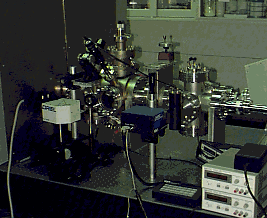
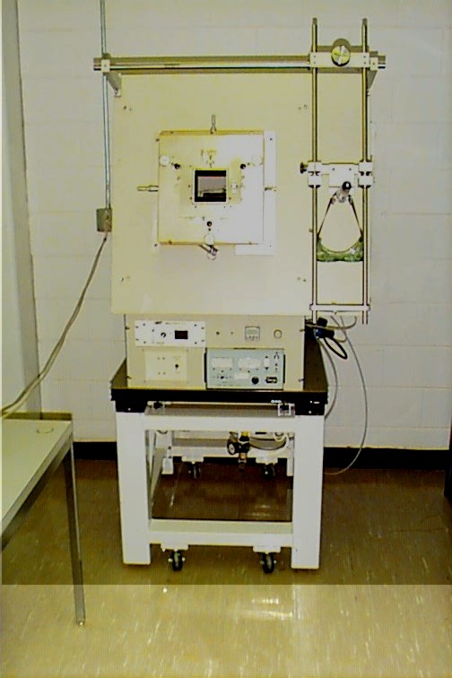
Molecular Beam Epitaxy (MBE) System used for deposition of novel EL phosphors
|
|
 |
|
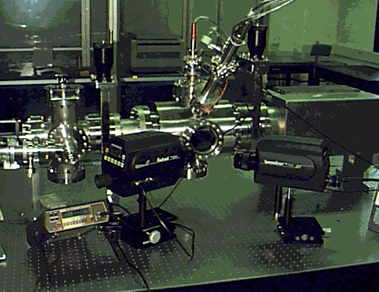
| To assess the quality of material layers, a variety of
material and surface characterization techniques are available. The capabilities
include Photoluminescence (PL), PL Excitation Spectroscopy (PLE), Charge
Deep Level Transient Spectroscopy (QDLTS), Secondary Ion Mass Spectrometry
(SIMS), Scanning Electron Microscopy (SEM), and X-ray diffractometry. Other
analytical instrumentation a Transmission Electron Microscope (TEM), an
Atomic Force Microscope (AFM), and X-ray crystallography equipment.
PTCOE's Automatic System of Materials Electrical Characterization (ASMEC) was specifically designed for electrical & photoelectric characterization of dielectric and wide gap semiconductors such as CaF2/ZnS/SrS. It uses powerful techniques such as Q-DLTS and Photo-stimulated Internal Field Transient Spectroscopy (PIFTS) to provide information on bulk/interface trap activation energies and capture cross sections, as well as trap concentration.
|
The photoluminescence spectroscopy system can be used to achieve above bandgap and direct excitationby deep- and/or mid UV lasers, a Xenon arc lamp and a Deuterium arc lamp. The resulting luminescence is analyzed with the detection system and provides information on the crystalline quality and impurities. In addition, a tunable light source allows PL excitation spectroscopy, which can be used to investigate the excitation mechanisms and the electronic structures of the luminescent centers in semiconductors. The dynamical properties of the luminescence such as excitation energy transfer can also be investigated by using pulsed lasers.
LIGHT SOURCES
|
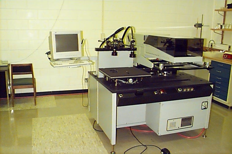
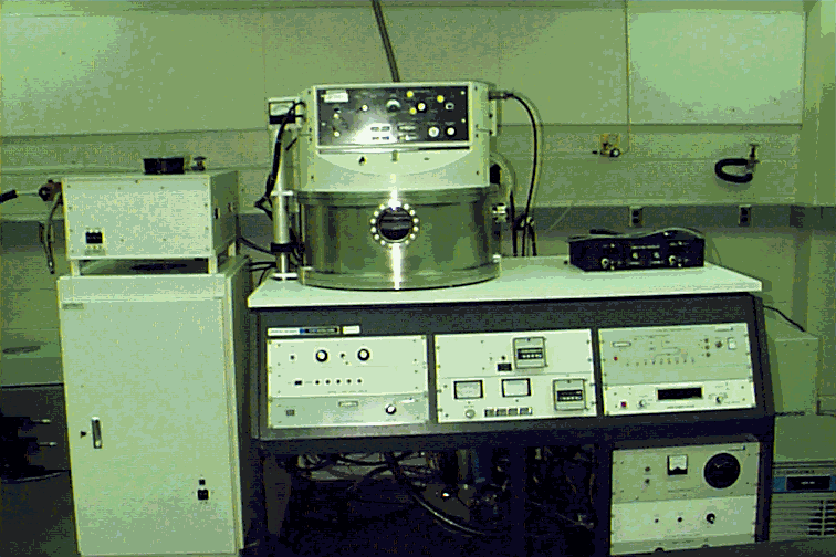
| To obtain accurate cathodoluminescent (CL) intrinsic efficiency
measurements, both the reflected and transmitted light components are measured
by employing a two-photometer system. This procedure provides an accurate
correction for the transmitted emission losses of different phosphors.
Both photometers sample the same excited area within the e-beam spot. A
Faraday cup is also used in the sample holder to determine the e-beam current
before the measurement. A fast response EFG-7F e-gun with a range from
0-5 kV is used for these measurements. The vacuum system has two viewports
available for the two photometers. Its transport arm is centered on the
beam axis, and a guide rail (which holds the rotation angle constant as
the samples are translated) is used. The transport arm can also be attached
to a motorized translation stage. This stage can be computer-controlled
to translate the samples across the e-beam automatically, and take the
measurements. The photometer also enables the sample chromaticity to be
obtained in the same measurement. In addition, the PMT/monochromator system
can be quickly put in place to measure the CL decay time of the different
phosphors using the E-gun in the pulsed mode. Decay times down to 50 ns
can be measured.
The saturation, transient analysis, and aging studies are conducted in a vacuum chamber equipped with Fison LEG 32 (0-5 kV) and LEG 320 (1-30 kV) E-guns. The LEG 32 has been well characterized for beam size and current density. A Faraday cup at the bottom of the chamber measures and monitors any changes in beam current. The LEG 320 gun is used for high energy intrinsic efficiency measurements, and in addition, provides a means for extracting diffusion length and surface recombination parameters.
|
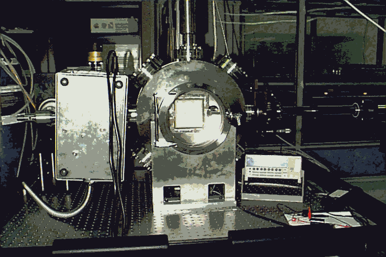
Cathodoluminescence Luminous Efficiency System
|
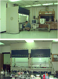
| PTCOE has access to Georgia Tech's Microelectronics
Research Center (MiRC), which is housed in a new (1989) 100,000 sq.ft.
building plus a 20,000 sq. ft. annex. MiRC includes six electronic and
optoelectronic materials labs, eight labs for microelectronic design and
testing, and eight labs for electronic device design and testing. A 7,000
sq.ft. cleanroom provides complete microfabrication facilities. Specialized
materials growth and vacuum deposition systems are also available for fabrication
of thin film semiconductor devices in a variety of material systems including
III-V and II-VI semiconductors. The photolithography area is a class 1000
room with specialized mask aligner exposure stations suitable for photolithography
into the submicron range. Other specialized equipments include surface
preparation systems and scanning electron microscopes.
Partial List of Cleanroom Equipment available at Georgia Tech's MiRC:
|
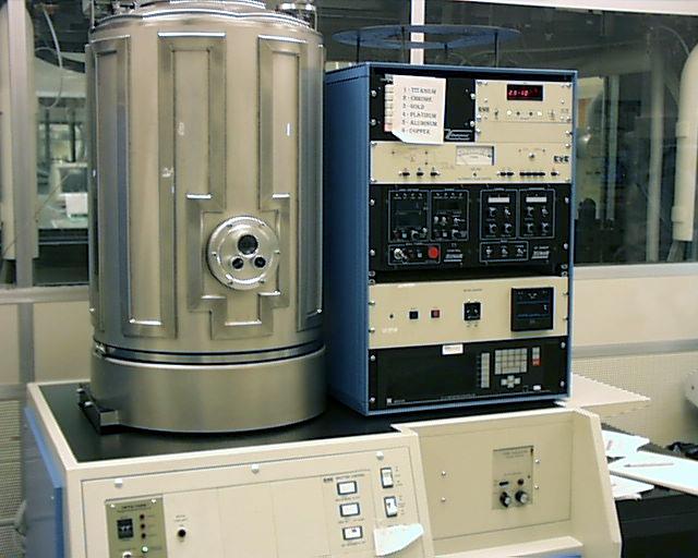
RF Sputtering System
|
PTCOE has extensive optical and electrical techniques for the analysis
and characterization of emissive and non-emissive displays as well as various
optoelectronic devices such as photodiodes and Light Emitting Diodes (LEDs).
Various computer-automated experiments are available to measure and analyze
the macroscopic & microscopic properties of thin-film heterostructure
devices. A practical probe test station has been designed and constructed
for electrical characterization measurements of optoelectronic and display
devices. Both high-voltage (150-250 V) and low-voltage (20-30 V) EL devices
can be investigated by applying unipolar and bipolar rectangular pulse
with different pulse widths. Two photometers (PR 650 & 880) are available
to measure device intensity (brightness) and CIE coordinates. A brief description
of some of these capabilities and the information they provide about the
device under test is presented in the table below.
|

Display & Device Characterization System
|
PTCOE has a suite of advanced semiconductor device simulation
tools (Silvaco's TCAD). These software packages contain both microscopic
as well as macroscopic device simulators, which provide a coupled, hierarchical
approach to semiconductor device modeling. Silvaco's device simulation
software uses powerful numerical techniques to solve for the various properties
of homojunction/heterojunction devices under different operating conditions.
A built-in optimizer allows for quick and accurate tuning of simulation
parameters. The following is an overview of the general capabilities of
Silvaco's ATLAS which includes the following tools and extensions:
PTCOE also employs Monte Carlo simulations in the analysis of CL phosphor properties, which incorporates the known physics of elastic and inelastic scattering processes for electrons incident on amorphous materials. The simulation reliably predicts range values for the primary electrons incident on the host and the electron range can be quickly calculated for many phosphors. |
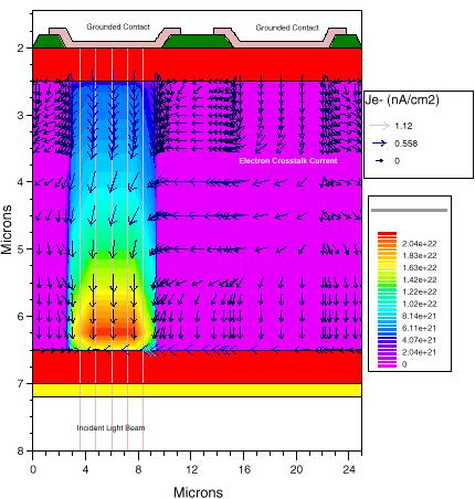
Two-dimensional Electrical/Optical Simulation of an Optoelectronic Device
|